
March 2020 Issue
Researcher Video Profiles
Tetsuo Kan Associate Professor Department of Mechanical and Intelligent Systems Engineering
MEMS technology for fabricating plasmonic devices
Tetsuo Kan is developing new MEMS devices or sensors, that is microelectromechanical systems which are based on semiconductor fabrication techniques.
"MEMS technology provides us with very small size sensors such as force sensors or inertial sensors or photodetectors and so on," says Kan. "We are focusing on new optical devices by combining MEMS and plasmonics."
Plasmonics is optical oscillation of metal nano or microstructures. So, if meal nano or microstructures are illuminated with light, then oscillation occurs on the surfaces of the metals.
But conventional methods for detecting these resonances use huge optical microscopes, and since such plasmonics is very sensitive to the external environment, and is a fascinating phenomenon for sensing.
"If we put such nanostructures on top of semiconductors such as MEMS, we can electrically detect oscillations as electrical signals," explains Kan. "So, we no longer require huge optical setups, so we can minimize plasmonic sensors within a very small chip size.So, we are applying this basic technology for developing new cost-effective photodetectors, or new spectrometers or new chemical sensors and so on."
The structures are made using microfabrication facilities at UEC Tokyo located in clean rooms build for nanolithography or photolithography.
In addition to microfabrication, optical simulation is also indispensable and in order to get very good resonant structures, Kan and his team carry out optical simulations to design high resonance structures and the fabrication process required. Kan refers to this as their "recipe for the microfabrication".
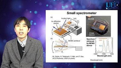
Recently, Kan has succeeded in making a new and very small spectrometer, based on a combination of the MEMS cantilever structures and a gold grating on the surface of a cantilever.
In this structure, gold gratings generate plasmonic resonance when the structure is illuminated by the light, and the plasmonic response is measured as a photocurrent on the surface of the cantilever.
Kan and his colleagues found that when the cantilever is vibrated and light is incident on the gold surface, they could retrieve spectrum information by calculating the relationship between the vibration angle and the photocurrent at each angle.
"We think that this is very small or one of the smallest spectrometers ever made," says Kan. "We are now applying this very small spectrometer to gas sensing, for example, in a room or in automotive environment, as new IoT sensor. I think the combination of MEMS and plasmonics is a novel approach to fabricate high performance and versatile sensors. So, I we will continue explore MEMS and plasmonics fields."
Further information
Research Highlight: MEMS technology for fabricating plasmonic near-infrared spectrometers
Department website: http://www.ms.mi.uec.ac.jp