
March 2017 Issue
News and Events
Harbin Engineering University students and faculty participate in international academic exchange on 'Advanced Photonics and Laser Technology' at UEC, Tokyo.
A delegation of eight outstanding students accompanied by three faculty members from Harbin Engineering University (HEU), College of Science, were invited to visit the University of Electro-Communications (UEC, Tokyo) to participate in a program, 'Advanced Photonics and Laser', held between 15 to 21 January 2017.
This program is jointly organized as a collaboration project by the Center for Photonic Innovation and Institute for Laser Science at UEC, Tokyo and the HEU College of Science. Furthermore, the program is also jointly supported by the Japan Science and Technology Agency (JST), the Japan-Asia Youth Exchange Program in Science, Sakura Science Plan.
On the first day, after the inauguration ceremony and ice-breaking session, an overview of the HEU College of Science's key research activities was given by the HEU School of Science Vice Dean, Professor Jianzhong Zhang. In the afternoon, the delegates visited the UEC Communication Museum to deepen their understanding of telecommunications and information technology. The museum houses a unique and valuable collection of telecommunications exhibits, ranging from early twentieth century telecommunications instruments to Japan's first nuclear magnetic resonance system and radio clock, both developed by UEC, Tokyo.
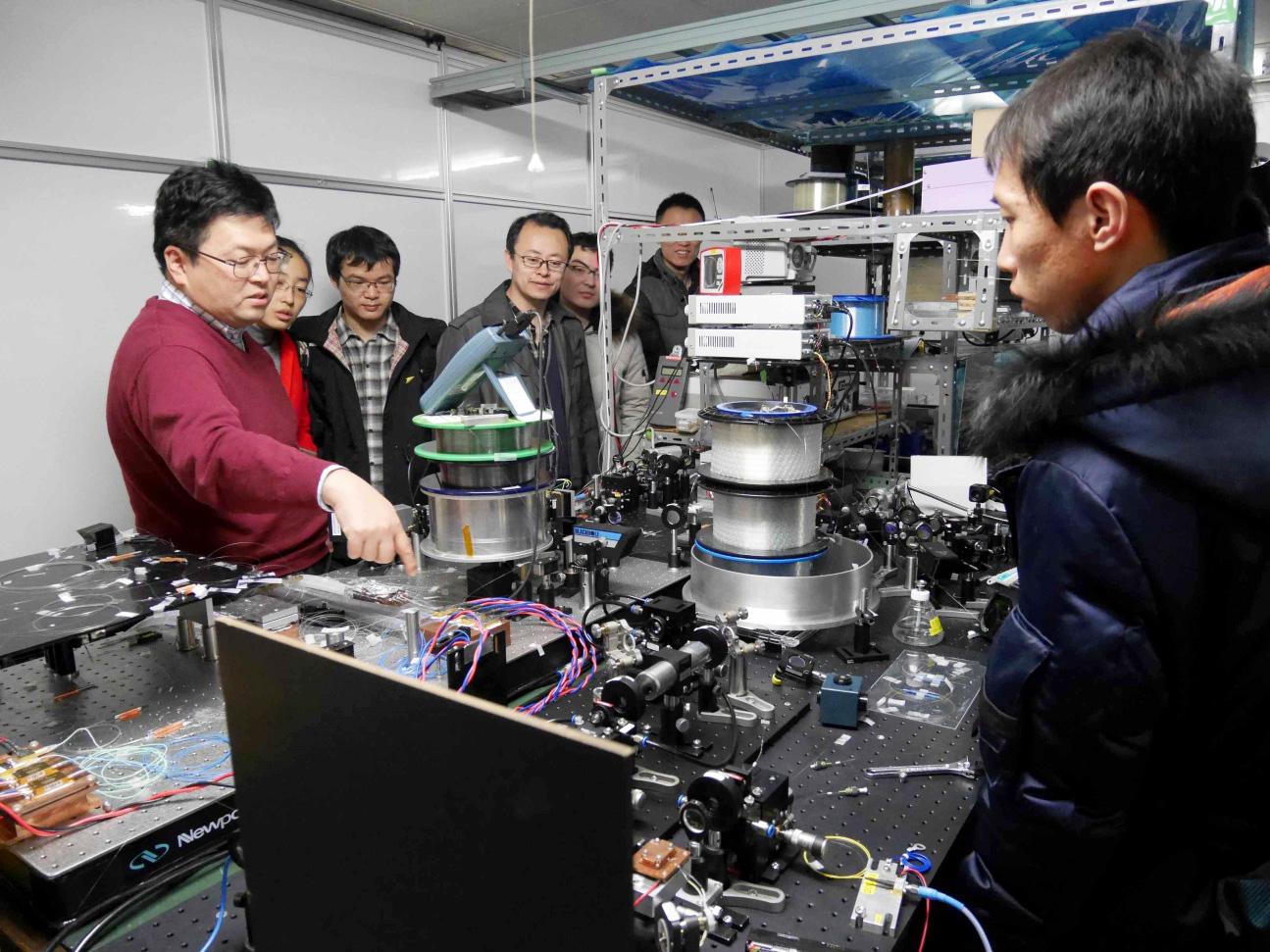
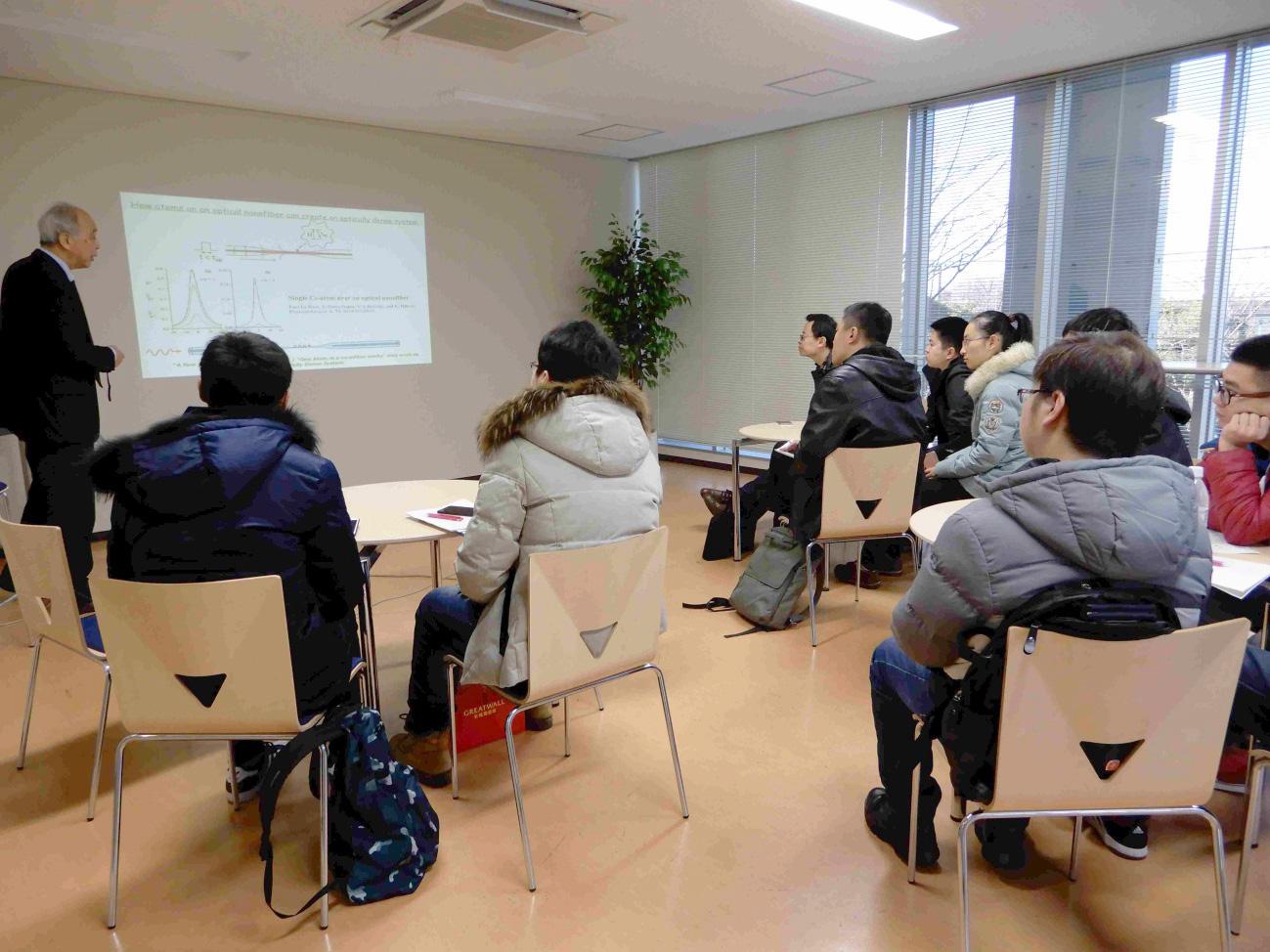
On the second day, the delegates visited the Center for Photonic Innovation and received a keynote lecture on "Development of Quantum Photonic and Nano Fiber" by Professor Kohzo Hakuta, Director of the Center for Photonic Innovation. In the afternoon, visitors were able to participate in experiments on advanced research photonic innovation under the guidance of researchers at the center. In the evening, the delegates walked to Jindaiji temple, near to UEC, Tokyo, to experience Japanese culture and enjoy the famous Jindaiji soba. It was a fulfilling day for both the hosts and visitors.
On the third day, UEC, Tokyo arranged a visit to the National Museum of Emerging Science and Innovation (Miraikan, Tokyo) and the Association for Technological Excellence Promoting Innovative Advances (TEPIA), to explore developments in the latest cutting-edge technology. During the trip, the participants experienced the cutting-edge science and learnt about Japan's outstanding exhibition methods of science. On the way to TEPIA, the delegates had stopped by the Gundam Front Tokyo in Odaiba, to see the iconic full-sized Gundam Statue and enjoy another kind of advanced science and technology in Japan.
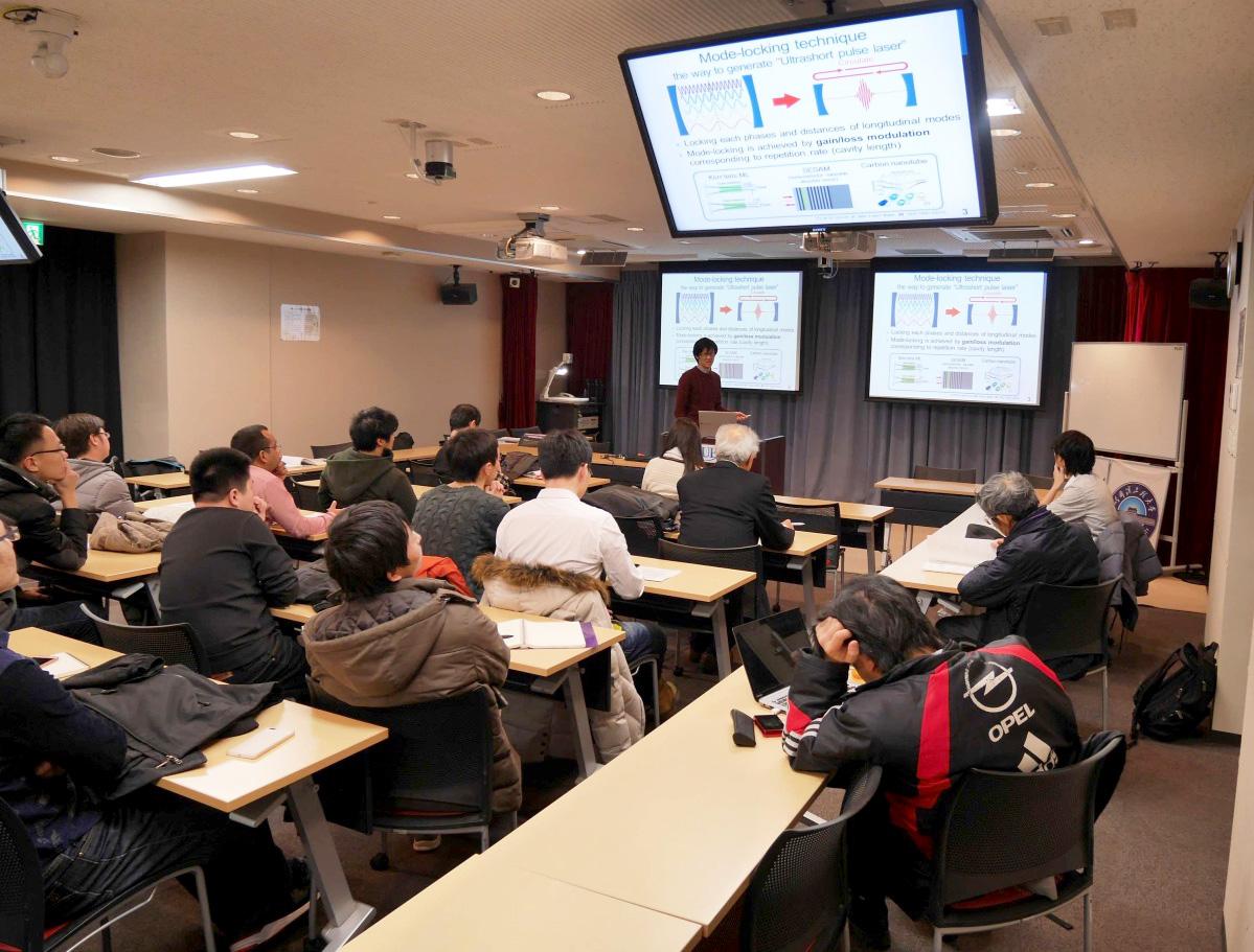
On the fourth day, the delegates visited the UEC, Tokyo, Institute for Laser Science, which is the only laser and atomic optical research facility in Japan, and internationally recognized for its contributions to laser science. The visit started with a brief overview of the institute's key projects, research activities and accomplishments by the center director Professor Hitoki Yoneda, followed by a laboratory tour of other groups (Shirakawa Laboratory, Musha Laboratory, Tokuragawa Laboratory, Katsuragawa Laboratory and Minoshima laboratory) affiliated with the center. The laboratory tour gave the delegates first-hand knowledge of the latest laser research including ultra-short pulse lasers, single frequency laser light source modulation, and optical combs (optical frequency comb).
On the final day of the program, a co-organized symposium on "Advanced Photonics and Laser" was held. Students and young researchers from both institutions actively participated in discussions on a wide range of topics, including laser sensing, fiber lasers, micro optical tweezers, quantum resonators by nanofibers, ultra-short pulse lasers, ultrafast attosecond pulse train, and optical combs. The speakers and title of talks are as follows:
Morning Session: Harbin University
- Yushi Chu, "Bismuthate related Active Medium"
- Zhangjun Yu, "Distributed Birefringence Dispersion Measurement for Polarization Maintaining Fibers"
- Min Zhang, "Single Fiber Optical Tweezers"
Afternoon Session: UEC Photonic Innovation Research Center and Institute for Laser Science (Hakuta Lab, Shirakawa Lab, Katsuragawa Laboratory, Minoshima Lab)
- Jameesh Keloth, "Fabrication of Photonic Crystal Nanofiber Cavities for Cavity QED"
- Shotaro Kitajima, "Ultrashort Pulse Laser based on New Ceramic Materials"
- Chuan Zhang, "Arbitrary Manipulation of Optical Amplitude and Phase and its Application to Generation of Ultrafast Atto Pulse Train"
- Akifumi Asahara, "Ultrafast Spectroscopy using Dual Optical Frequency Combs"
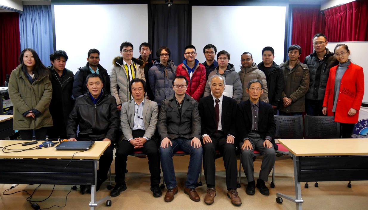
After the symposium, the participants gathered for a farewell dinner. In addition to acknowledging their participation in the program, the delegates also received a Sakura Science Plan completion certificate from Professor Kohzo Hakuta.
This program enabled friendly, engaging, and productive discussion between students and faculty members from both institutions. The UEC, Tokyo organizers look forward to continued collaboration with Harbin Engineering University in the future.