Research HighlightsResearch
October 2024 Issue
ElectronicsLayer-by-layer copper aluminum oxide films for advanced p-type thin film transistors
As the basic building blocks of many electronic devices, transistors are an integral part of our society. A particularly widely used type of transistor is the field-effect transistor, in which an electric field is used to control the current in a semiconductor — a material that doesn’t conduct current as well as copper and other metals but is also not an insulator like glass. The control of current flow in the semiconductor enables the amplification of electric signals. Field-effect transistors are commonly used to amplify weak signals, for example in wireless communication technologies. Research on transistors is on-going, as fabricating materials for novel transistors, which typically need to be highly crystalline and defect-free, can be challenging. Now, Hideo Isshiki and colleagues from The University of Electro-Communications, Tokyo have succeeded in manufacturing a thin film transistor (TFT) based on copper aluminum oxide (CAO), with initial tests showing promising device characteristics. TFT is a key device for flexible and transparent electronics.
Most field-effect transistors are of the so-called n-type, meaning that the relevant charge carriers are electrons, which are negatively charged. Transistors in which positively charged ‘holes’ — local electron deficiencies — conduct the current are known as p-type. Generally, electrons are more mobile than holes, which is one of the reasons n-type TFTs are more commonly used. Yet, p-type TFTs are also valuable for complementary MOS(CMOS) system contributing to low power consumption, which is why Isshiki and colleagues aimed to develop a p-type TFT that can be relatively easily manufactured and has good device characteristics.
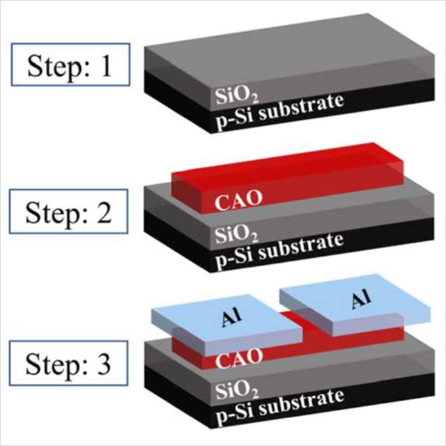
The researchers used a technique called layer-by-layer sputtering, a method enabling the deposition of atoms onto a substrate in a well-controlled manner. The carefully timed successive release of copper, aluminum and oxygen atoms onto a silicon oxide substrate, followed by thermal treatment, resulted in orderly stacked layers of copper oxide and aluminum oxide. The crystallinity, morphology and chemical composition of the CAO thin film were checked by means of various analytical techniques, including x-ray diffraction and electron microscopy, and found to be excellent. Overall structural integrity of the CAO film is important for achieving higher hole mobility and therefore enhanced electric conductivity.
Isshiki and colleagues then fabricated a TFT by depositing aluminum electrodes on top of the CAO-on-substrate structure. Device characteristics were measured and confirmed to correspond to typical p-type behavior. An important characteristic is the field effect mobility, which was found to be 4.1 cm² per volt per second. This value is promising, but the scientists believe it is still possible to improve it by eliminating certain crystallinity issues — a more precisely controlled thermal process may facilitate this.
An important aspect of the research reported by Isshiki and colleagues is that the sputtering process involved digital pulse patterns — the sputter release of atomic material was programmed as the repetition of an optimized cycle — which enables the formation of highly crystalline layered structures. Quoting the scientists: “[Our] layer-by-layer approach offers a promising pathway for controlled stacking deposition routes in the growth of CAO thin films, enabling enhanced performance and device integration.”
References

Mehdi Ali, Daiki Yamashita, Hideo Isshiki, Growth of CuAlO2 on SiO2 under a layer-by-layer approach conducted by digitally processed DC sputtering and its transistor characteristics, Jpn. J. Appl. Phys. 63, 035502 (2024).
- URL : https://doi.org/10.35848/1347-4065/ad2aa5
- DOI : 10.35848/1347-4065/ad2aa5
Isshiki Lab website
http://www.flex.es.uec.ac.jp/