Research HighlightsResearch
October 2023 Issue
Turing patterns go nano
The formation of certain patterns in nature, such as particular animal skin stripes or spots, can be explained by means of reaction–diffusion theory. This formalism, developed by Alan Turing, is based on the presence of two components (called ‘activator’ and ‘inhibitor’) with different diffusion rates. These two-component situations can give rise to what is collectively known as Turing patterns, such as the stripes seen on the skin of tropical fish or emerging order in chemical systems. Typical length scales of biological Turing patterns range from millimetres to centimetres. For purely chemical systems, the characteristic lengths are usually sub-millimetre. Although reaction–diffusion theory does not pose limits on intrinsic length scales, Turing patterns on the nanometre scale are rare. Recently, however, Yuki Fuseya from the University of Electro-Communications, Tokyo, and colleagues have identified a new type of nanoscale Turing patterns in a monolayer of bismuth atoms on a substrate.
The patterns had been observed earlier, when scientists tried growing atomic monolayers of bismuth (Bi) on niobium diselenide (NbSe2); such materials are investigated for their promising electronic properties. Fuseya and colleagues were intrigued by the mysterious patterns seen in these Bi/NbSe2 systems, in the form of ripples, as they resembled the Y-shaped arrangement of stripes on angelfish. What is remarkable is that the monolayer stripe patterns are more than a million times smaller than the fish patterns.
Fuseya and colleagues built a model describing how Bi atoms arrange themselves on a NbSe2 substrate. The height of a Bi atom is the variable determining the ripple pattern, consisting of ‘peaks and ‘valleys’. The researchers found that it is not enough to include elastic interactions between Bi atoms and adsorption interactions between Bi atoms and the NbSe2 substrate in the model: orientational effects in the Bi–Bi interactions have to be taken into account as well— specifically, the angles between Bi–Bi bonds.
The dynamics of the set of Bi atoms could then be described by an equation of motion for the displacements of the atoms. Numerical evaluations of the equation led to various types of ripple patterns, including the Y-shaped arrangements seen in the earlier experiments, with an intrinsic length (between peaks or valleys) of five times the interatomic Bi distance. The scientists then checked whether their model could be interpreted as a reaction–diffusion situation. They were indeed able to rewrite the system’s equation of motion as a reaction–diffusion equation, with a Bi atom’s vertical displacement (perpendicular to the NbSe2 substrate) as the activator, and the horizontal displacement (parallel to the substrate) as the inhibitor.
The researchers then tested what happened when a pattern was perturbed. They observed self-restoration of the original pattern, thus recovering the ‘wound healing’ property of reaction–diffusion systems. Finally, they studied the effect of applying strain to the system, and showed that doing so can change the Bi atom patterns in a controlled way.
The findings of Fuseya and colleagues are of particular importance as they demonstrate the existence of Turing patterns in ‘hard condensed matter’, which are moreover expected to have practical relevance. Quoting the researchers, “[the] obtained patterns can prove to be building blocks for new devices or new physics that have been unexplored”.
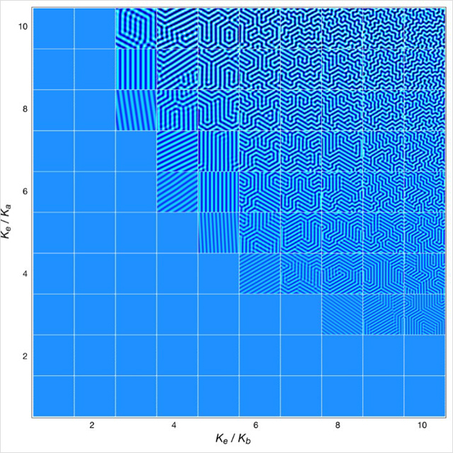
Caption: Various nanoscale Turing patterns of bismuth atoms on a substrate.
References
Yuki Fuseya, Professor, Department of Engineering Science
Yuki Fuseya, Professor, Department of Engineering Science
Yuki Fuseya, Hiroyasu Katsuno , Kamran Behnia and Aharon Kapitulnik , Nanoscale Turing patterns in a bismuth monolayer, Nature Physics 17, 1031–1036 (2021).
- URL : https://www.nature.com/articles/s41567-021-01288-y
- DOI : 10.1038/s41567-021-01288-y